Overview
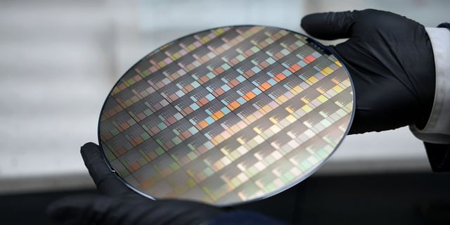
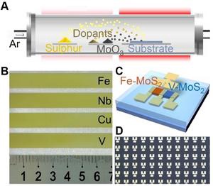
- A novel metal-assisted van der Waals epitaxy method produced four-inch monolayer MoS₂ films with precise transition-metal substitutional doping and atomic-scale uniformity.
- Fe-doped MoS₂ transistors delivered electron mobilities up to 71.2 cm²/V·s and on/off ratios beyond 10⁸, with roughly 265,000 top-gate devices integrated on a single wafer showing consistent performance.
- CDimension’s proprietary CVD process enables direct growth of monolayer MoS₂ on silicon at about 200 °C without harming underlying circuits, paving the way for 3D stacking of 2D devices.
- Researchers predict these wafer-scale 2D processes could meet the power, performance and footprint requirements of future sub-1 nm (10A) logic nodes.
- Key hurdles remain in scaling defect-free large-area films and adapting fabrication workflows for full-scale integrated circuit production.