Overview
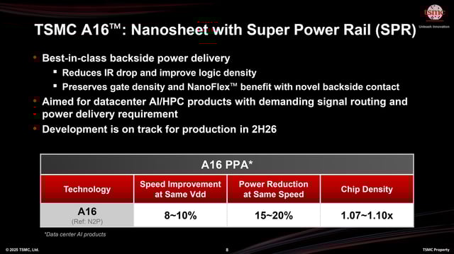
- TSMC's A14 process, set for mass production in 2028, offers up to 15% faster performance or 30% lower power consumption compared to its upcoming N2 node.
- The A14 node features 2nd Generation gate-all-around nanosheet transistors and NanoFlex Pro for optimized power, performance, and design flexibility.
- The new System on Wafer-X packaging technology will integrate up to 16 large computing chips, memory, and optical interconnects for advanced AI applications.
- TSMC is on track to begin high-volume production of its 2nm N2 node in the second half of 2025, marking a major milestone in its roadmap.
- Apple, Nvidia, and AMD are expected to benefit significantly from TSMC's advancements, with the A14 node likely to enhance AI and device performance in future products.