
Overview
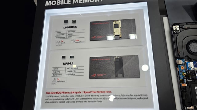
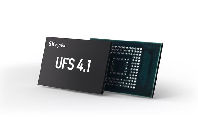
- SK hynix has introduced its UFS 4.1 storage solution, built on the world’s first 321-layer 1 terabit NAND flash technology.
- The chip offers a 7% improvement in power efficiency and a reduced thickness of 0.85 mm, tailored for ultra-slim smartphones and AI-powered devices.
- It achieves the fastest sequential read speeds for fourth-generation UFS at 4,300 MB/s, alongside 15% and 40% improvements in random read and write speeds, respectively.
- Sample shipments are planned for late 2025, with mass production expected to begin in the first quarter of 2026 in 512GB and 1TB capacities.
- SK hynix is also advancing the development of SSDs based on the same 321-layer NAND for both consumer and data center applications, targeting completion by the end of 2025.