
Overview
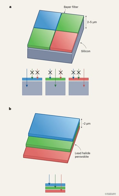
- Each perovskite sensor stacks red-, green- and blue-sensitive layers in a vertical arrangement, eliminating the need for lossy optical filters.
- These thin films feature pixel dimensions between 0.5 and 1 millimeter, showcasing a transition from proof of concept toward practical device scales.
- Laboratory tests indicate these sensors can theoretically capture three times more light and deliver triple the spatial resolution of silicon counterparts.
- The materials’ tunable halide compositions enable customized absorption bands, opening the door for hyperspectral imaging in medical diagnostics and environmental monitoring.
- Researchers plan to reduce pixel sizes to the micrometer range and to develop specialized readout electronics that accommodate perovskite’s unique semiconductor properties.