

Overview
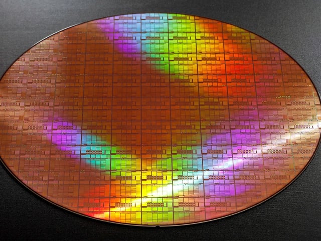
- Rapidus has started prototyping 2nm gate-all-around wafers at its IIM-1 facility in Hokkaido to validate its process technology in early test runs.
- Initial test wafers are achieving expected electrical benchmarks across key performance parameters, confirming that fab tools and process settings are operating as planned.
- The IIM-1 plant has integrated over 200 advanced DUV and EUV lithography tools to support precision patterning and generate high-resolution data for AI-driven yield improvements.
- The company is committing to single-wafer processing for every front-end step, enabling real-time adjustments, enhanced defect monitoring and faster process optimization.
- Rapidus aims to deliver a 2nm process development kit in the first quarter of 2026 and scale full 2nm mass production by 2027 to join Samsung and TSMC in leading-edge chip manufacturing.