Overview
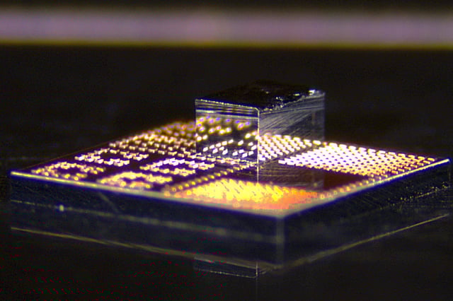
- Researchers fabricate microscopic GaN dielets on a GaN wafer and use a specialized vacuum tool to bond them onto silicon CMOS substrates with nanometer precision.
- The copper-to-copper bonding forms below 400 °C, cutting integration costs and preserving material integrity compared to traditional gold-based methods.
- Prototype hybrid power amplifiers delivered stronger RF signals, broader bandwidth and cooler operation than equivalent all-silicon devices.
- Distributing discrete GaN transistors across the silicon chip surface reduces hotspots and leverages existing semiconductor foundry procedures.
- The hybrid chips promise advances in wireless communications and radar systems, smartphone call quality and battery life, and could support quantum computing at cryogenic temperatures.