Overview
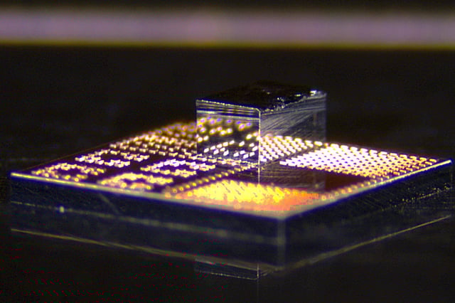
- Researchers fabricate microscopic GaN transistor dielets on a GaN wafer and then transfer them onto standard silicon CMOS dies using low-temperature copper-to-copper bonding.
- A specialized tool aligns GaN dielets with nanometer precision and applies heat and pressure below 400 °C to preserve material integrity.
- Prototype power amplifiers made with these hybrid chips deliver higher bandwidth and gain than devices built with traditional silicon transistors.
- Distributing discrete GaN transistors across the silicon surface enhances heat dissipation and lowers overall system temperature.
- The process’s compatibility with standard semiconductor foundries paves the way for improved smartphone connectivity, expanded wireless bandwidth and quantum computing applications.