Overview
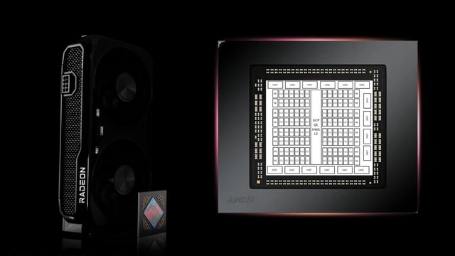
- Block diagrams shared by leaker Kepler_L2 depict four next-gen AMD GPUs with 96, 40, 24 and 12 compute units.
- The top die is shown with eight shader arrays, 16 shader engines and 16 unified 32-bit memory controllers for a potential 512-bit interface, with coverage noting up to 128 MB of Infinity Cache.
- The 40‑CU design is pictured with six memory controllers implying a 192‑bit bus, while the 24‑CU and 12‑CU dies show eight and four controllers respectively, with some reports suggesting LPDDR5X for lower tiers.
- Outlets reconcile earlier 192‑CU rumors by reporting a shift in AMD’s counting such that one new CU roughly corresponds to a previous‑gen WGP, making 96 “new” CUs akin to 192 by the old measure.
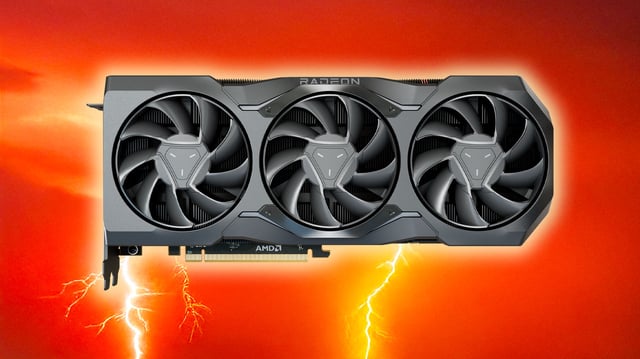
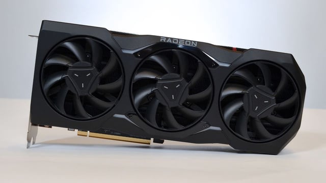
- Reporting frames all specifications as leak-driven and subject to change, with mass production expected around Q2 2026 and talk of AMD preparing a genuine high-end option to challenge Nvidia remaining speculative.