

Overview
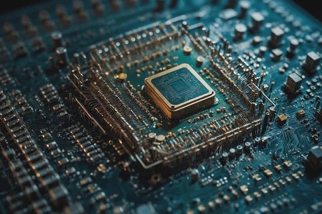
- Union Minister Ashwini Vaishnaw inaugurated India’s first 3 nm chip design centres in Noida and Bengaluru, marking a leap in domestic design capabilities.
- The facilities are part of the India Semiconductor Mission, launched in December 2021 with a Rs 76,000 crore outlay to build end-to-end chip fabrication, testing, packaging and design capacity.
- Major fabrication and assembly/testing projects worth over Rs 1.55 lakh crore—including Micron’s Rs 22,516 crore site in Sanand and a Rs 91,000 crore Tata Electronics–Powerchip fab in Dholera—are advancing across Gujarat, Uttar Pradesh and Assam.
- Under the Design-Linked Incentive scheme, Rs 234 crore has been approved for 22 startups developing chipsets for mobile networks, satellite communications, power management and imaging, with one venture focused on 3 nm designs.
- Talent development is scaling up through SMART Lab training for more than 100,000 engineers and through global partnerships as India prepares to host over 300 exhibitors at SEMICON India 2025.